Monocrystalline silicon is the foundation of modern semiconductor and photovoltaic industries. To transform silicon ingots into functional wafers, precision cutting is essential. Among various cutting technologies, diamond wire saw cutting (DWS) has become the industry standard due to its efficiency, precision, and minimal material loss.
In this comprehensive guide, we will explore the monocrystalline silicon cutting process, focusing on diamond wire saw cutting machines, their working principles, advantages, and industry applications.

Before diving into the cutting process, let’s briefly discuss monocrystalline silicon and why it requires specialized cutting techniques.
1.1 What is Monocrystalline Silicon?
Monocrystalline silicon is a highly pure form of silicon with a single, continuous crystal lattice structure. It is produced using the Czochralski (CZ) method or the Float Zone (FZ) method, resulting in cylindrical ingots.
1.2 Why Precision Cutting is Critical
– Semiconductor Industry: Silicon wafers must have ultra-smooth surfaces(nanometer-level roughness) for microchip fabrication.
-Photovoltaic Industry: Solar cells require thin, uniform wafers(typically 160-180µm) to maximize efficiency.
– Minimal Kerf Loss: Reducing material waste during cutting improves cost efficiency.
Traditional cutting methods like ID saws (inner diameter saws) and multi-wire slurry saws have been replaced by diamond wire saw cutting** due to superior performance.
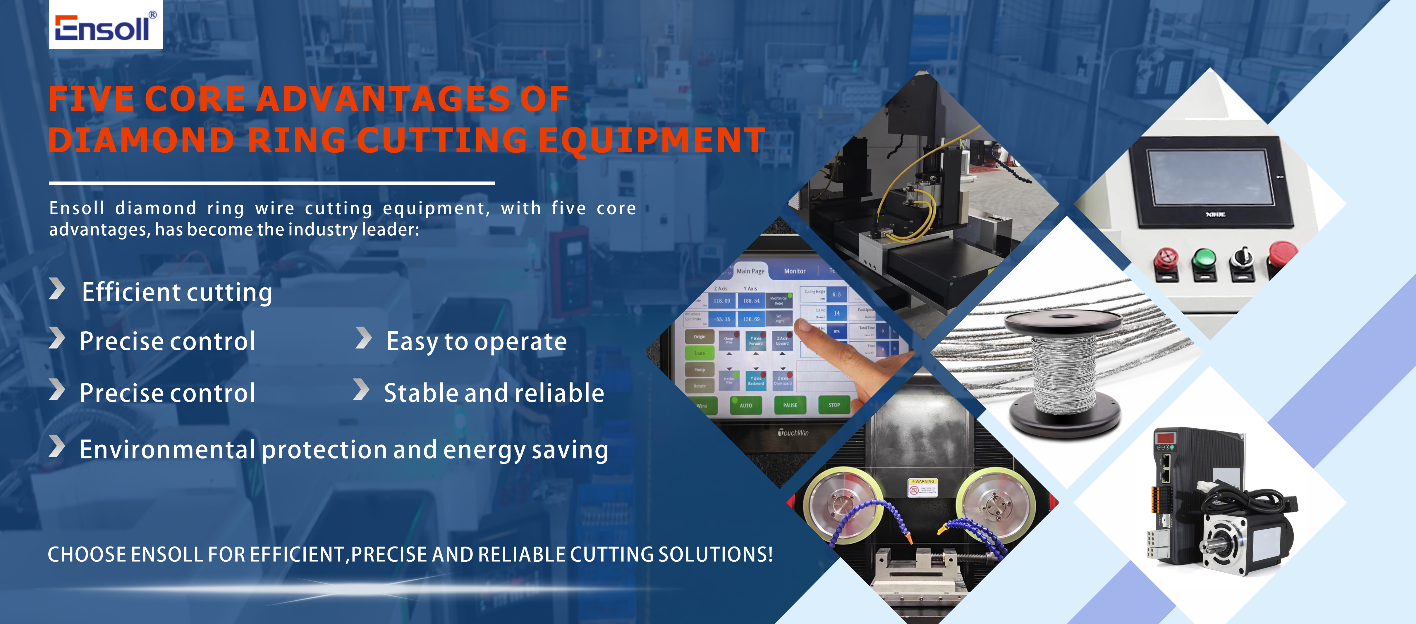
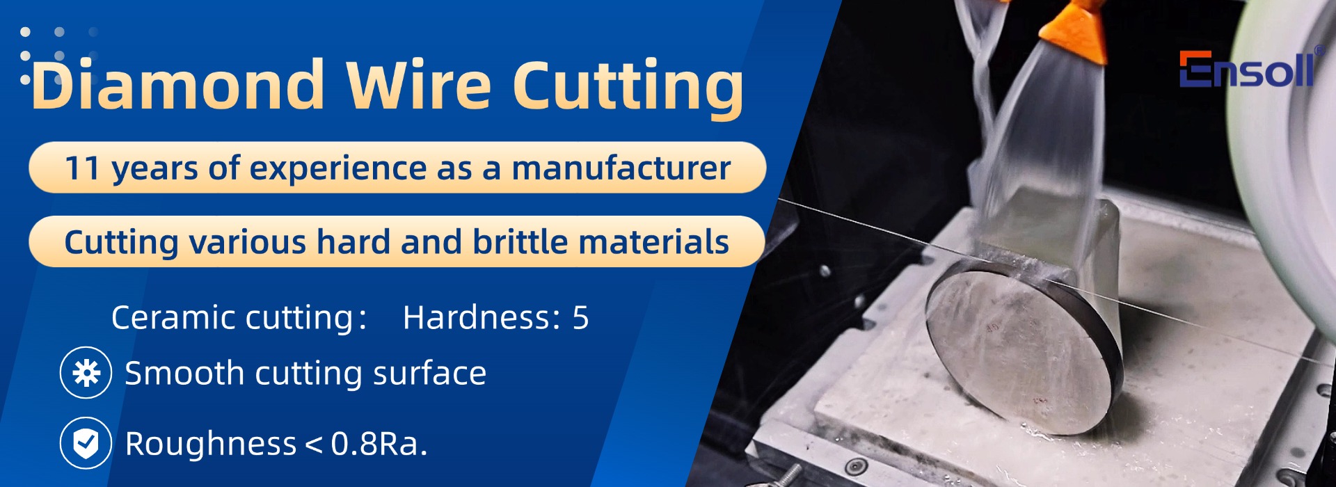
A diamond wire saw (DWS) cutting machine uses a high-tensile steel wire embedded with diamond abrasive particles to slice through hard materials like silicon. The wire moves at high speeds (10-15 m/s) while the workpiece is fed into it, enabling precision cutting with minimal kerf loss.
2.2Key Components of a Diamond Wire Saw Machine
2.3 How Diamond Wire Saw Cutting Works
3.Advantages of Diamond Wire Saw Cutting
Compared to older methods like multi-wire slurry saws (MWSS), DWS offers:
3.1 Higher Cutting Speed & Efficiency
– Cutting speeds up to 1.5x faster than slurry-based methods.
– Multi-wire configurations allow simultaneous cutting of hundreds of wafers.
3.2 Reduced Kerf Loss & Material Waste
– Kerf width as low as 120-150µm (vs. 180-220µm in slurry saws).
– Higher yield per ingot, crucial for cost-sensitive solar manufacturing.
3.3 Improved Surface Quality
– Lower subsurface damage (SSD) due to controlled abrasive action.
– Reduced wire marks and waviness, minimizing post-cutting polishing.
3.4 Environmental & Cost Benefits
– No slurry disposal issues (unlike MWSS, which uses abrasive slurry).
– Longer wire lifespan (up to 1,000 cuts per wire).

Despite its advantages, DWS faces some challenges:
– Cause: Excessive tension, abrasive wear, or coolant failure.
– Solution: Real-time tension monitoring**, optimized diamond grit size, and proper coolant filtration.
4.2 Surface Micro-Cracks
– Cause: Brittle fracture during cutting.
– Solution: Controlled feed rate, post-cut etching, or annealing.
4.3 Wire Bow Effect
– Cause: Uneven wire tension leading to wavy cuts.
– Solution: Advanced wire guidance systems with dynamic tension control.
5.1 Photovoltaic (PV) Industry
– Solar wafer production (Mono PERC, TOPCon, HJT cells).
– Thin-wafer cutting (below 150µm for next-gen high-efficiency cells).
5.2 Semiconductor Industry
– Silicon wafer dicing for IC manufacturing.
– Advanced packaging** (e.g., wafer-level packaging).
5.3 Other Applications
– LED sapphire substrate cutting.
– Hard material machining (SiC, quartz, ceramics).
Diamond wire saw cutting has revolutionized monocrystalline silicon wafer manufacturing, offering superior precision, efficiency, and cost savings over traditional methods. As the semiconductor and solar industries push for thinner, larger wafers, DWS technology will continue to evolve, enabling next-generation electronics and renewable energy solutions.
For manufacturers, investing in advanced diamond wire saw machines is critical to staying competitive in the high-tech materials market.
If you have any question, please contact us